MINAMI Co., Ltd. headquater
Void-less Reflow 【Pattented】
In the LSI’s mounted on the latest electronic equipment such as the cellular phones, a lot of surface mounting BGA packages and chip size packages are used.
When the bumps for BGA and CSP are formed by the printing method, the ball shaped bumps are formed by printing the solder paste on the wafer and melting the solder particles in the paste in the reflow oven.
Now that the Pb free solder has become popular and the bumps are becoming finer, solder joint defect caused by air bubbles (void) generated in the bumps has become a problem.
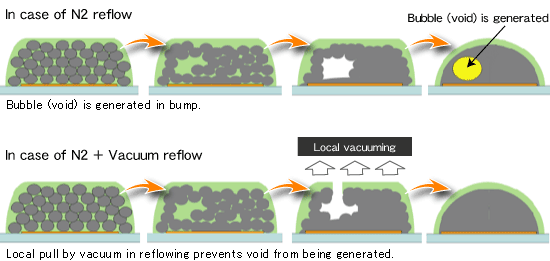
In the case of MINAMI reflow oven, the solder is melted in vacuum environment in the main zone.
When the solder melting temperature is reached, the solder will change from powder to liquid, and the alloy becomes a fluid. By heating and vacuuming the wafer at that timing, gas inside the solder is sucked out. This process helps to lessen the voids in comparison to the conventional N2 reflow oven.
- Solder melting image
- Comparisons between N2 reflow and N2 + vacuum reflow
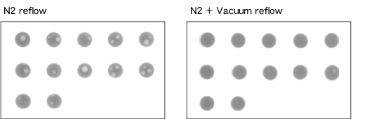
There is no bubble generated in N2 + vacuum reflow as seen on the right、 whereas white bubbles are seen in the N2 reflow.
-
In the case of Minami reflow oven with vacuum, the wafer traveling range is kept within a circle of 1.8 meter diameter. Therefore, it is easy to maintain air tightness, and oxygen can be reduced to 50ppm or less by filling N2 gas. And generation of oxide film can be suppressed, and production in low oxygen environment is possible. In addition to the air tightness, vacuum void-less function is equipped in the reflow zone. Air bubbles (voids) in BGA and CSP, which basically could not be reduced in the past, can be eliminated by sucking in the vacuum chamber, and uniform bumps without voids can be formed.
Copyright© 2013 MINAMI Co.,Ltd. All rights reserved.